

Computer assisted design (CAD) has completely transformed the way that we design just about everything. Products can now be designed and developed in ways that simply weren’t possible before. CAD software gives designers a clear visual representation of what their product is going to look like before a machine actually produces it.

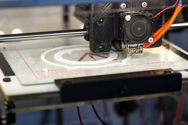
Now that 3D printing is beginning to mature as a technology, CAD is becoming more versatile and has advanced rapidly in recent years. It’s now possible to place a physical object in a box, scan it with lasers, and have a 3D printer replicate it.
PCBs and CAD
CAD has been used for some time in the design of printed circuit boards (PCBs), which are used in the majority of modern consumer electronics. There are lots of different CAD software out there to choose from, and there’s even some software you can use for free! While all the CAD options, paid or otherwise, do more or less the same thing, the interfaces and specific feature sets will be different.
One thing to consider is that some electronic CAD software allows the user to install custom plugins. These can add features and tools, in some cases radically changing the capabilities of the software. The best software for you will depend on exactly what you want to do with it. If you want to produce PCBs, Altium is worth checking out. If you’re completely new, try out Design Spark to get a general feel for CAD software.
Schematic Capture
Designing a PCB using CAD begins with a process known as ‘schematic capture’. This involves mapping the components’ positions on the circuit board and deciding on the connections that will link them together. A schematic is like a blueprint; it shows the overall architecture of the circuit board and shows its functionality.
Another term you should know is ‘nets’. Nets are the electrical traces on the schematic that join the components together. Electricity will flow through the net in order to make the circuit board function.
Turning a Schematic Capture Into a Circuit
Once a schematic has been designed, it then needs to be tested. Testing is usually also done using software whenever possible. Most PCB design software also enables the user to test their circuit before they proceed to printing and assembly.
During this process, the positions of the components and internal copper connections are finalized. Using the ‘switch to board’ mode that most PCB design software offers, designers can place components directly on a virtual board, as well as name them and give them values.
For any hobbyist who works with electronics, an understanding of PCBs will open new worlds to you. If you want to work on more advanced projects, you will need to be able to design simple circuits to underpin them. The availability of free PCB design software means that you can try it out for yourself for free. Or, if you’re already familiar with CAD software but haven’t designed PCBs before, try out a premium software package like Altium.


