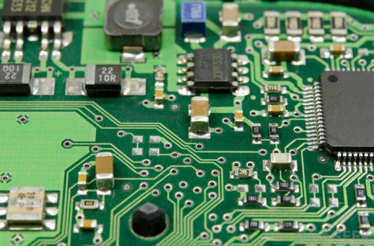
Remember repairing damaged printed circuit board pads is a fragile task! Before starting this you should know what exactly is this connected pad of PCB! It can be described as a part of PCB in which pins of several other connectors like chips, transistors, etc are attached. Commonly it is seen that during any breakage of the device or in the case of removal of any components from the Printed Circuit Board, it lead to damaging the connected parts. You can learn more about PCBs from this url.
There are certain things that you should have before you have made up your mind to repair a PCB. The list of these elements are as follows:
- Clean, lint-free cloth
- Flux
- A microscope and if you have magnifying glasses then it works wonders
- Soldering iron and solder
- C-clamps
- Handful of Toothpicks
- Wipes and isopropyl alcohol
- A safe, flat- polished ESD cutting surface
- X-Acto knife
- Adhesive copper tape
- Circuit frame
Now when you have all the materials to do this repair you can start with the steps to repair PCB pads.
The steps to repair damaged printed circuit board pads are simple to follow.
PCB is designed by sticking the layers of copper and several fiber glasses together. The glues which are utilized here to put this layer together are extremely heat resistant and hence it is not recommended to overheat it as you may end up damaging it. Certain brands are designed so well with better pads and tracks that they sustain in long run without a chance of PCB trace repair.
There are several instances where when PCB was overheated, the results were very disheartening. The layer of copper that is added there gets de-laminated and detached from the circuit board. The joints get ruptured and circuits may become dysfunctional. There are possibilities to repair damaged printed circuit board pads with solder and adhesive copper tape by following some simple steps:
- Clean the place that is ruptured- try to remove the slightest possible damage to get the desired sound back. It is advisable to cut the area that has been damaged with a sharp knife or any sharp object so that no additional damage happens during the removal.
- Clean the area that is ruptured- after cleaning the damaged portion, the remaining areas become clear.
- Expose the track- take a sharp object like a sharp knife or screwdriver, and in case if you have none then you can use good quality sandpaper. Make the open area lustrous and clean. If there are any remaining portions even after cleaning it is advisable to burn the PCB material so that it doesn’t act as a hindrance while sticking the tape.
- Apply copper tape on the reveal area- cover the rupture area by overlapping the track by sticking some copper tape on it.
- Fastening the ends with copper tape- fasten the rupture joints where the repair is needed. Generally, the copper adhesive tape melts when the temperature increases so it is advisable to use very light heat while putting it on the ruptured ends. After cooling this tape turns more sticky.
- Punch in between to make a hole- start by rubbing the padded area with a circled, tough item. It will help the copper tape to get inside the padded area, easily. The hole that is made in the pad will be visible through this tape and later simply punch with any pointed item like a needle, paper clip, or other such things.
- Connecting the elements carefully- elements here are connected swiftly in a normal way. Pass the heat as little as possible while introducing the new pad as it is too sensitive.
- Be careful while trimming- you need to be very careful while cutting the copper tape and remember to use craft knife or sharp scissors while cutting it. It will be easy for you to cut the unwanted portion of the tape or the extra portion with it. Repairing is a very careful task and if you are careful while doing it then you may avoid future problems or repairing.


